Glass substrates may be the next big thing in chips; Apple looking

Share via:


A new supply-chain report suggests that Apple is seeking to be an early player in what some believe will be the next big thing in chip development: printed circuit boards (PCBs) made from glass substrates.

While that might not sound exciting, it offers the prospect of an entirely new way of mounting and packaging chips, which could offer much better thermal performance, allowing processors to run at maximum power for longer periods …

Glass substrates can boost chip performance

Current PCBs are typically made from a mix of fibreglass and resin beneath the copper and solder layers.

The material is sensitive to heat, which means that chip temperatures have to be carefully controlled through thermal throttling: reducing the performance of the chip when it gets too hot. This means chips can only sustain their maximum performance for limited periods, before falling back to slower speeds to keep temperatures down.

Switching to glass would substantially increase the temperatures the board can be subjected to, which in turn means that chips can run hotter, and therefore maintain peak performance for longer.

Glass substrates are also ultra-flat, allowing for more precise engraving, which allows components to be placed closer together, increasing the density of circuits within any given size.

Intel currently holds the lead in this field, but other companies are working hard to catch up.

Apple in discussion with suppliers

Digitimes reports that Samsung is now working on this technology, and that Apple is in discussion with several unnamed suppliers – with Samsung certain to be among them.

Subsidiaries of the Samsung Group will collaborate to invest in the research and development of Glass Core Substrates (GCS) to expedite their commercialization, aiming to rival Intel, which has taken an early lead in this sector […]

Apple is reportedly in discussions with several companies to devise a strategy for incorporating glass substrates into electronic devices. The adoption of glass substrates by Apple in the future is expected to significantly broaden the scope of application areas.

Sources within the semiconductor industry indicated that glass substrates may become a new field for completion among nations, attracting participation from global IT device manufacturers and semiconductor players in addition to substrate manufacturers.

Samsung is well-placed to work on this, as many of the techniques used in manufacturing advanced, multilayered displays are also applicable to making glass substrate PCBs.

Potentially the next big thing, but with challenges

The reason some believe that glass substrates will be the next big thing in chip development is that most progress to date has been achieved through ever-smaller processes. Apple currently leads the way with the 3nm chip in the A17 Pro powering the iPhone 15 Pro models, with plans for 2nm and then 1.4nm.

Each successive process generation is harder and harder to achieve, with ultimate physical limits to just how small we can go. With doubts as to how long Moore’s Law will remain in effect, some believe that new materials hold the key to maintaining the pace of development as we begin reaching the limits of process size.

However, there are big challenges ahead, as SemiEngineering explains.

“Think about glass as a means to get interconnect density very similar to what you would get with silicon interposers,” says Rahul Manepalli, fellow and director of substrate TD module engineering at Intel. “A glass substrate gives you that capability, but it comes with very challenging integration and interface engineering problems that we have to solve.”

Some of these challenges include fragility, a lack of adhesion to metal wires, and difficulties in achieving uniform via fill, which is crucial for consistent electrical performance. In addition, glass presents unique challenges for inspection and measurement, due to its high level of transparency and differing reflective indices compared to silicon. Many measurement techniques that work on opaque or semi-transparent materials are less effective on glass. For instance, optical metrology systems that rely on reflectivity to gauge distance and depth must adapt to glass’ translucency, which can cause signal distortion or loss, compromising measurement accuracy.

“All of these technologies assume certain physics,” says John Hoffman, computer vision engineering manager at Nordson Test & Inspection. “When you start changing substrates, will the physics still work? And can you recover? A lot of our algorithms make certain assumptions about the physics. Do those algorithms still work, or do we have to come up with brand new algorithms because the physics has changed?”

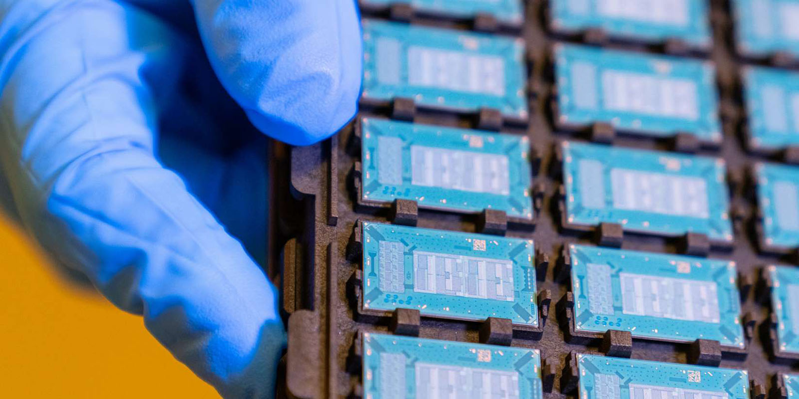
Photo: Intel

FTC: We use income earning auto affiliate links. More.


Source link

Disclaimer

We strive to uphold the highest ethical standards in all of our reporting and coverage. We StartupNews.fyi want to be transparent with our readers about any potential conflicts of interest that may arise in our work. It’s possible that some of the investors we feature may have connections to other businesses, including competitors or companies we write about. However, we want to assure our readers that this will not have any impact on the integrity or impartiality of our reporting. We are committed to delivering accurate, unbiased news and information to our audience, and we will continue to uphold our ethics and principles in all of our work. Thank you for your trust and support.

Popular

More Like this

Glass substrates may be the next big thing in chips; Apple looking


A new supply-chain report suggests that Apple is seeking to be an early player in what some believe will be the next big thing in chip development: printed circuit boards (PCBs) made from glass substrates.

While that might not sound exciting, it offers the prospect of an entirely new way of mounting and packaging chips, which could offer much better thermal performance, allowing processors to run at maximum power for longer periods …

Glass substrates can boost chip performance

Current PCBs are typically made from a mix of fibreglass and resin beneath the copper and solder layers.

The material is sensitive to heat, which means that chip temperatures have to be carefully controlled through thermal throttling: reducing the performance of the chip when it gets too hot. This means chips can only sustain their maximum performance for limited periods, before falling back to slower speeds to keep temperatures down.

Switching to glass would substantially increase the temperatures the board can be subjected to, which in turn means that chips can run hotter, and therefore maintain peak performance for longer.

Glass substrates are also ultra-flat, allowing for more precise engraving, which allows components to be placed closer together, increasing the density of circuits within any given size.

Intel currently holds the lead in this field, but other companies are working hard to catch up.

Apple in discussion with suppliers

Digitimes reports that Samsung is now working on this technology, and that Apple is in discussion with several unnamed suppliers – with Samsung certain to be among them.

Subsidiaries of the Samsung Group will collaborate to invest in the research and development of Glass Core Substrates (GCS) to expedite their commercialization, aiming to rival Intel, which has taken an early lead in this sector […]

Apple is reportedly in discussions with several companies to devise a strategy for incorporating glass substrates into electronic devices. The adoption of glass substrates by Apple in the future is expected to significantly broaden the scope of application areas.

Sources within the semiconductor industry indicated that glass substrates may become a new field for completion among nations, attracting participation from global IT device manufacturers and semiconductor players in addition to substrate manufacturers.

Samsung is well-placed to work on this, as many of the techniques used in manufacturing advanced, multilayered displays are also applicable to making glass substrate PCBs.

Potentially the next big thing, but with challenges

The reason some believe that glass substrates will be the next big thing in chip development is that most progress to date has been achieved through ever-smaller processes. Apple currently leads the way with the 3nm chip in the A17 Pro powering the iPhone 15 Pro models, with plans for 2nm and then 1.4nm.

Each successive process generation is harder and harder to achieve, with ultimate physical limits to just how small we can go. With doubts as to how long Moore’s Law will remain in effect, some believe that new materials hold the key to maintaining the pace of development as we begin reaching the limits of process size.

However, there are big challenges ahead, as SemiEngineering explains.

“Think about glass as a means to get interconnect density very similar to what you would get with silicon interposers,” says Rahul Manepalli, fellow and director of substrate TD module engineering at Intel. “A glass substrate gives you that capability, but it comes with very challenging integration and interface engineering problems that we have to solve.”

Some of these challenges include fragility, a lack of adhesion to metal wires, and difficulties in achieving uniform via fill, which is crucial for consistent electrical performance. In addition, glass presents unique challenges for inspection and measurement, due to its high level of transparency and differing reflective indices compared to silicon. Many measurement techniques that work on opaque or semi-transparent materials are less effective on glass. For instance, optical metrology systems that rely on reflectivity to gauge distance and depth must adapt to glass’ translucency, which can cause signal distortion or loss, compromising measurement accuracy.

“All of these technologies assume certain physics,” says John Hoffman, computer vision engineering manager at Nordson Test & Inspection. “When you start changing substrates, will the physics still work? And can you recover? A lot of our algorithms make certain assumptions about the physics. Do those algorithms still work, or do we have to come up with brand new algorithms because the physics has changed?”

Photo: Intel

FTC: We use income earning auto affiliate links. More.


Source link

Disclaimer

We strive to uphold the highest ethical standards in all of our reporting and coverage. We StartupNews.fyi want to be transparent with our readers about any potential conflicts of interest that may arise in our work. It’s possible that some of the investors we feature may have connections to other businesses, including competitors or companies we write about. However, we want to assure our readers that this will not have any impact on the integrity or impartiality of our reporting. We are committed to delivering accurate, unbiased news and information to our audience, and we will continue to uphold our ethics and principles in all of our work. Thank you for your trust and support.

Website Upgradation is going on for any glitch kindly connect at office@startupnews.fyi

More like this

FInd your lost wallet with your iPhone using SwitchBot...

I have an AirTag on my keychain to...

M4 MacBook Pro teardown reveals nearly identical internals to...

While the new M4 MacBook Pros got a...

Apple @ Work: Understanding Apple’s Private Wi-Fi Address feature

Apple @ Work is exclusively brought to you...

Popular

Upcoming Events

Startup Information that matters. Get in your inbox Daily!