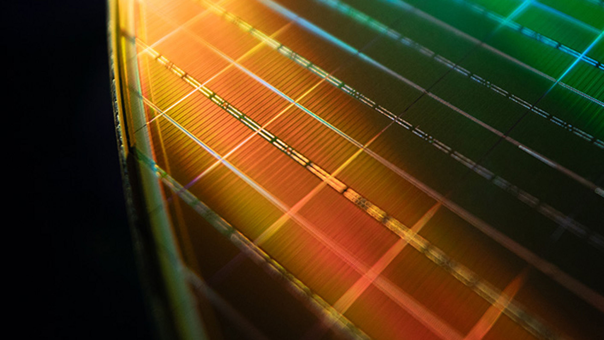
The Institute of Microstructure Physics of the data-analytics-id=”inline-link” href=”http://www.ipmras.ru/” data-url=”http://www.ipmras.ru/” target=”_blank” referrerpolicy=”no-referrer-when-downgrade” data-hl-processed=”none”>Russian Academy of Sciences (via data-analytics-id=”inline-link” href=”https://x.com/torgeek/status/1971504406991609885″ data-url=”https://x.com/torgeek/status/1971504406991609885″ target=”_blank” referrerpolicy=”no-referrer-when-downgrade” data-hl-processed=”none”>Dmitrii Kuznetsov) has laid out a long-term roadmap for domestic extreme ultraviolet (EUV) lithography tools operating at a wavelength of 11.2 nm, extending the information the organization data-analytics-id=”inline-link” href=”https://www.tomshardware.com/tech-industry/russia-plans-euv-chipmaking-tools-that-it-says-will-be-cheaper-and-easier-to-build-than-asmls-country-outlines-new-roadmap-to-smaller-chips” data-before-rewrite-localise=”https://www.tomshardware.com/tech-industry/russia-plans-euv-chipmaking-tools-that-it-says-will-be-cheaper-and-easier-to-build-than-asmls-country-outlines-new-roadmap-to-smaller-chips”>shared last December. The new project spans from 2026, utilizing 40nm manufacturing technology, and extends to 2037, incorporating sub-10nm fabrication processes. The latest roadmap looks more realistic than some previous ones, yet it…


![[CITYPNG.COM]White Google Play PlayStore Logo – 1500×1500](https://startupnews.fyi/wp-content/uploads/2025/08/CITYPNG.COMWhite-Google-Play-PlayStore-Logo-1500x1500-1-630x630.png)