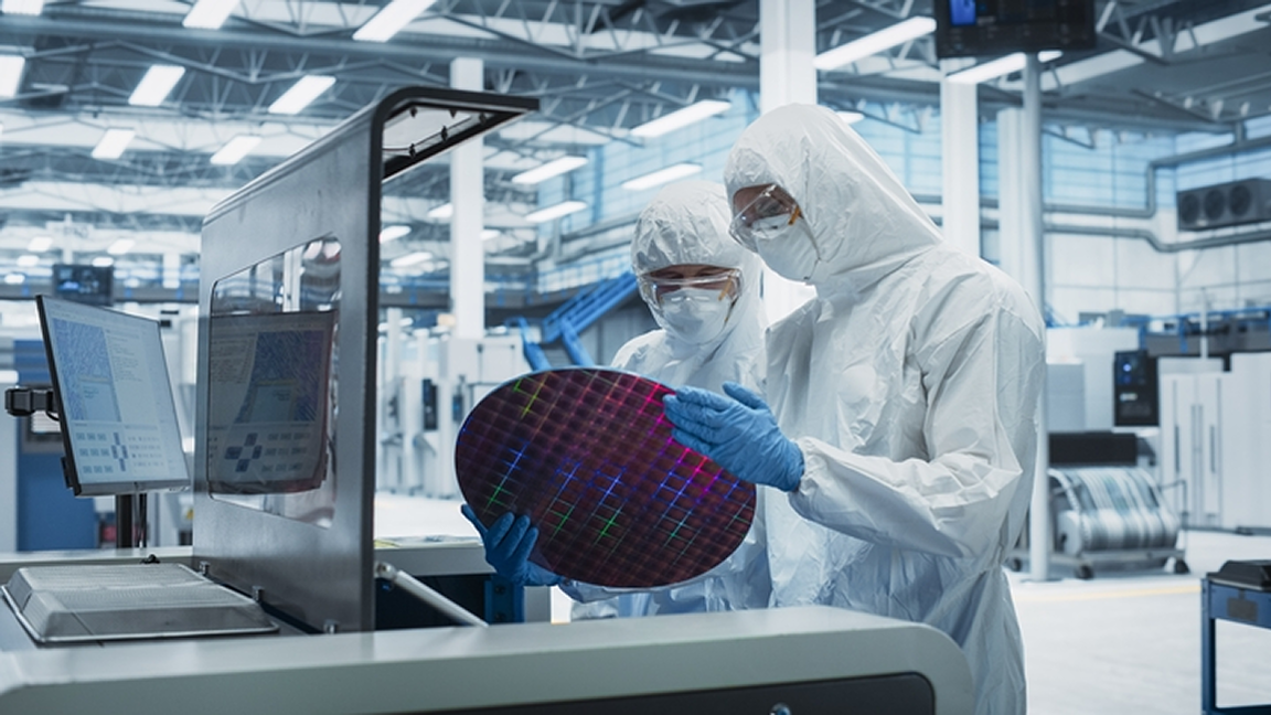
The Substrate startup has been data-analytics-id=”inline-link” href=”https://www.tomshardware.com/tech-industry/semiconductors/american-startup-substrate-promises-2nm-class-chipmaking-with-particle-accelerators-at-a-tenth-of-the-cost-of-euv-x-ray-lithography-system-has-potential-to-surpass-asmls-euv-scanners” target=”_blank” data-before-rewrite-localise=”https://www.tomshardware.com/tech-industry/semiconductors/american-startup-substrate-promises-2nm-class-chipmaking-with-particle-accelerators-at-a-tenth-of-the-cost-of-euv-x-ray-lithography-system-has-potential-to-surpass-asmls-euv-scanners”>doing the rounds in the news lately, thanks to its proposition of making chips using particle accelerators and X-rays instead of conventional EUV lithography, claiming it can eventually have angstrom-sized features at only $10,000 per wafer—in U.S. fabs, no less. Those are bold claims, and data-analytics-id=”inline-link” href=”https://substack.com/home/post/p-177604037″ target=”_blank” data-url=”https://substack.com/home/post/p-177604037″ referrerpolicy=”no-referrer-when-downgrade” data-hl-processed=”none”>an article by Fox Chapel Research (FCR) is seriously questioning whether they pay off.
The write-up is the first of two parts, and takes aim at not just the seemingly outlandish…


![[CITYPNG.COM]White Google Play PlayStore Logo – 1500×1500](https://startupnews.fyi/wp-content/uploads/2025/08/CITYPNG.COMWhite-Google-Play-PlayStore-Logo-1500x1500-1-630x630.png)