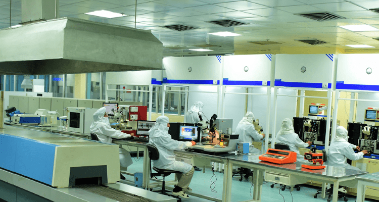
India has opened a large semiconductor prototyping hub to help researchers and startups move chip designs from lab to fabrication faster, strengthening domestic capabilities.
India’s semiconductor ambitions are shifting from policy announcements to physical infrastructure.
A national research agency has opened a major chip prototyping hub designed to help engineers, startups, and academic teams test and validate chip designs before full-scale manufacturing. The facility addresses one of the biggest bottlenecks in India’s semiconductor push: the long and expensive path from design to fabrication.
The hub is intended to serve as a shared resource, lowering barriers for teams that lack access to advanced testing and prototyping tools.
Why prototyping matters
Designing a chip is only the first step. Before fabrication, designs must be verified, tested, and iterated—often multiple times—to catch flaws that could make production runs unusable.
In countries with mature semiconductor ecosystems, prototyping infrastructure is deeply embedded. In India, that gap has forced many designers to rely on overseas partners, adding cost, delay, and dependency.
By centralizing prototyping capabilities, the new hub aims to shorten development cycles and keep more of the value chain onshore.
A strategic complement to fabrication plans
India has announced incentives to attract chip fabs, but fabs alone do not create an ecosystem. Without strong design, validation, and packaging capabilities, manufacturing remains vulnerable.
The prototyping hub complements fabrication efforts by strengthening upstream capabilities. It also supports India’s sizable chip design talent pool, which has historically worked for global companies rather than domestic manufacturers.
For policymakers, the logic is clear: retaining intellectual property matters as much as producing silicon.
Startups and researchers stand to benefit most

Early-stage chip startups often struggle to secure prototyping access, especially when competing with larger clients at overseas facilities. Academic teams face similar constraints.
A shared national hub can level that playing field, allowing smaller players to test ideas without committing to prohibitively expensive fabrication runs.
That access could be critical in emerging areas such as power electronics, automotive chips, and specialized processors.
A long-term investment
The hub will not make India a semiconductor powerhouse overnight. Prototyping is one piece of a complex puzzle involving supply chains, skills, and global partnerships.
But it marks a tangible step toward reducing dependence on foreign infrastructure—and toward building a more resilient domestic chip ecosystem.
In semiconductors, progress is measured in decades. This is one of those foundational moves.