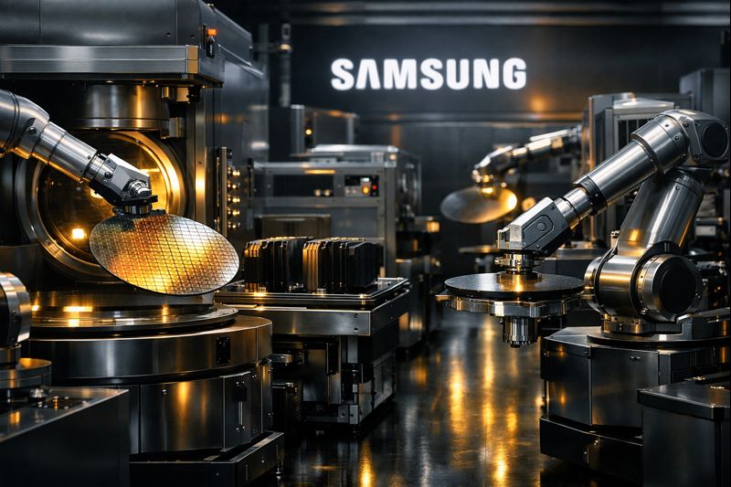
Samsung plans a major Gwangju investment, establishing an advanced semiconductor packaging facility to strengthen its AI chip supply chain capabilities.
Samsung Electronics is reportedly poised to make a significant strategic investment in Gwangju, South Korea, with plans to establish a new advanced semiconductor packaging facility. This move signals a profound commitment to bolstering its capabilities in a critical segment of the artificial intelligence (AI) chip supply chain, a sector experiencing exponential growth and intense competition.
The potential investment, expected to be unveiled at an upcoming meeting between South Korean President Lee Jae Myung and the heads of the nation's largest conglomerates, underscores Samsung's determination to accelerate spending and solidify its position in the rapidly evolving semiconductor landscape. This is not merely an expansion; it represents a calculated maneuver in the high-stakes game of AI dominance, where advanced packaging has emerged as a pivotal battleground.
The New Frontier of Semiconductor Innovation: Advanced Packaging
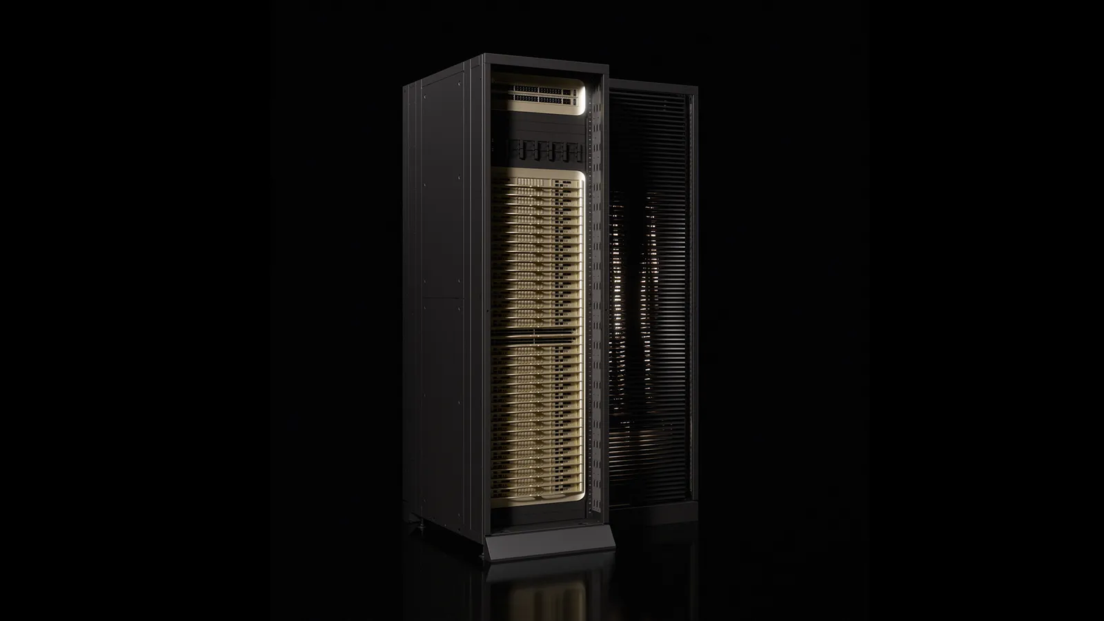
For decades, the semiconductor industry's relentless pursuit of performance was primarily driven by shrinking transistor sizes, adhering to Moore's Law. However, as the physical limits of silicon fabrication approach, advanced packaging has emerged as the next frontier for enhancing chip performance, power efficiency, and cost-effectiveness. It involves integrating multiple chips or chiplets into a single package, creating a highly complex, three-dimensional system.
This shift is particularly pronounced in the realm of AI. Modern AI workloads, from large language models to complex machine learning algorithms, demand immense computational power and, crucially, high-bandwidth memory (HBM). HBM chips stack multiple DRAM dies vertically, dramatically increasing memory bandwidth while reducing the physical footprint. The ability to efficiently integrate these HBM stacks with powerful AI processors, such as those from Nvidia or AMD, is where advanced packaging becomes indispensable.
This investment by Samsung is a clear recognition of the industry's trajectory. The value chain for high-performance computing is no longer solely about fabricating the silicon wafer; it extends critically into how those chips are assembled and interconnected. Mastery of advanced packaging techniques can provide a significant competitive edge, dictating not just performance metrics but also time-to-market for next-generation AI accelerators.
Samsung's Strategic Imperative and Market Dynamics
Samsung Electronics is a dominant player in memory chips and a significant player in foundry services. However, in the burgeoning HBM market, it faces stiff competition, particularly from domestic rival SK Hynix, which has historically held a larger share. This proposed packaging facility is a direct response to that dynamic, positioning Samsung to strengthen its HBM capabilities and vertically integrate its offerings for AI customers. The company recently announced it began shipping samples of its latest HBM chip, the 12-layer HBM4E, to customers, indicating its aggressive push.
Samsung's move signals confidence in the long-term growth of the AI sector and the company's commitment to capturing a larger piece of this lucrative market. The anticipated upswing in the chip sector, largely fueled by AI demand, makes such infrastructure investments crucial. Companies that can offer a comprehensive solution, from silicon fabrication to advanced packaging and memory, are likely to command premium pricing and stronger customer relationships. This investment can be seen as a de-risking strategy, ensuring Samsung controls a vital part of the supply chain rather than relying solely on external partners for packaging services.
The global semiconductor market is experiencing a fundamental reorientation around AI. This has led to an explosion in demand for specialized hardware, and packaging is no longer an afterthought but a co-design imperative. The move by Samsung aligns with a broader industry trend where integrated device manufacturers (IDMs) and even pure-play foundries are heavily investing in advanced packaging to offer complete solutions.
Connecting the Dots: Broader Industry Trends and Geopolitical Stakes
This development is not isolated; it connects to several significant trends shaping the global technology landscape. Firstly, it underscores the intensifying "chip war" narrative, where nations are vying for self-sufficiency and leadership in semiconductor manufacturing. South Korea, like the U.S., Europe, and Japan, views semiconductor dominance as a matter of national security and economic prosperity. Investment in advanced packaging plants within national borders contributes to supply chain resilience and reduces reliance on potentially vulnerable overseas facilities.
Secondly, it reflects the increasing complexity and cost of chip design and manufacturing. As traditional scaling becomes more challenging, companies are turning to heterogeneous integration—combining different types of chiplets (e.g., CPU, GPU, memory, I/O) from various process nodes into a single package. This modular approach allows for greater flexibility, higher yield, and optimized performance, making advanced packaging a crucial enabler for next-generation systems.
Samsung's expanded capabilities translate into more reliable access to cutting-edge components for those developing AI hardware or software. A robust and diverse supply chain for advanced packaged chips can mean quicker iteration cycles, potentially lower costs in the long run, and access to more powerful hardware platforms. The ability to integrate HBM with advanced processors is no longer a niche requirement; it's becoming a standard for competitive AI solutions, impacting everything from data centers to autonomous systems.
Samsung’s proposed advanced packaging facility in Gwangju exposes a critical reality: Silicon Fabrication is no longer the sole bottleneck in the AI revolution. As Moore’s Law stutters, 3D chip stacking, which is essential for the new 12-layer HBM4E memory, is the only way to deliver the massive bandwidth required by next-generation AI models. Samsung is aggressively playing catch-up against TSMC’s dominant CoWoS technology and SK Hynix’s grip on the HBM market. While offering a vertically integrated, "One-Stop-Shop" for giants like Nvidia and Google is strategically sound, capital alone won't erase TSMC's multi-year head start. For Samsung, flawless execution in advanced packaging has shifted from a Competitive Advantage to an Existential Requirement.
The improvements delivered by advanced packaging are tangible for enterprise customers deploying AI models or end-users interacting with AI-powered applications. Faster processing, lower latency, and enhanced energy efficiency translate into more responsive AI services, longer battery life for devices, and more powerful computing experiences. The seamless interaction between high-bandwidth memory and processing units, facilitated by sophisticated packaging, is fundamental to the smooth operation of generative AI applications and complex simulations.
Challenges and the Path Forward
While the strategic benefits are clear, Samsung's journey in advanced packaging is not without its challenges. The technology itself is incredibly complex, requiring significant R&D investment, specialized equipment, and highly skilled talent. Competing against established leaders like TSMC, which has a significant head start in various advanced packaging technologies (e.g., CoWoS), will require sustained effort and innovation.
Moreover, the capital expenditure required for such facilities is astronomical, necessitating careful financial planning and a robust pipeline of customer commitments. The semiconductor industry is cyclical, and while AI demand appears strong, overcapacity can become an issue. Samsung's ability to differentiate its packaging offerings and secure long-term contracts with major AI players like Nvidia, AMD, and Google will be crucial for the success of this venture.
My read on this development is that Samsung is making a decisive move to secure its long-term relevance in the AI era. By investing heavily in advanced packaging, they are not just reacting to market demand; they are proactively shaping their future as an integrated provider of critical AI components. The race for AI supremacy is multifaceted, and mastering the physical integration of chips is as important as designing them. This facility in Gwangju could become a cornerstone of Samsung's strategy to move beyond memory leadership and establish itself as an end-to-end powerhouse for AI silicon solutions.
The coming years will see intense competition and innovation in advanced packaging, and Samsung's investment positions it squarely at the forefront of this crucial technological evolution, with implications reaching across the entire global technology ecosystem.
Frequently asked questions
Where is Samsung considering building its new chip packaging plant?
Samsung Electronics is reportedly planning to establish its new advanced semiconductor packaging facility in Gwangju, South Korea. This strategic investment aims to bolster its capabilities in the AI chip supply chain.
What is the purpose of Samsung's new chip packaging plant?
The new plant is intended to strengthen Samsung's position in the critical segment of the artificial intelligence (AI) chip supply chain. It signifies a profound commitment to advanced semiconductor packaging capabilities.
What segment of the tech industry will this plant support?
This plant will specifically support the rapidly growing artificial intelligence (AI) chip supply chain. It's a critical investment in a sector experiencing exponential growth and intense competition.
Why is chip packaging important for AI?
Advanced chip packaging is crucial for AI chips as it allows for higher performance, better power efficiency, and more compact designs, which are essential for complex AI computations and integration.
What is the significance of Gwangju for this investment?
Gwangju, South Korea, is the chosen location for this significant strategic investment. Its selection likely involves factors such as existing infrastructure, talent pool, and government incentives to support the advanced semiconductor industry.
How will this impact Samsung's competition?
By bolstering its advanced packaging capabilities, Samsung aims to enhance its competitive edge in the highly contested AI chip market. This move could solidify its leadership and supply chain resilience against rivals.