A Chinese startup claims the world's first 8-inch 2D semiconductor pilot line, potentially revolutionizing post-silicon electronics from smartphones to AI.
A Chinese startup is making waves in the global semiconductor industry with a bold claim: it has established the world's first 8-inch pilot production line for two-dimensional (2D) semiconductors. This development could represent a significant step forward in the quest for post-silicon electronics, potentially impacting everything from the smartphones in our pockets to the advanced AI systems driving future technologies, and it puts a spotlight on the ongoing innovation race.
Here's why this matters: while an 8-inch wafer might sound modest compared to the 12-inch wafers common in today's leading-edge silicon fabs, scaling 2D materials like graphene or molybdenum disulfide (MoS2) to this size for manufacturing is an immense technical hurdle that has largely confined them to laboratory research. This purported breakthrough signals a potential shift from theoretical promise to industrial viability, particularly in a landscape dominated by traditional silicon technology.
For decades, silicon has been the undisputed king of semiconductors, powering virtually every electronic device. However, as chips become smaller and more powerful, silicon is bumping up against fundamental physical limits, making further miniaturization incredibly challenging and expensive. This has fueled a global hunt for alternative materials that can continue the march of technological progress, often referred to as the "More than Moore" era.
The Chinese startup's announcement, while lacking extensive public details, points to a determined effort to leapfrog existing semiconductor paradigms. Creating an 8-inch wafer for these atomically thin materials means tackling complex issues like uniform deposition, defect control, and integration at a scale that begins to approach commercial manufacturing, a challenge that has stymied researchers and companies worldwide.
Why 2D Semiconductors Are a Big Deal
At their core, 2D semiconductors are materials that consist of a single or just a few layers of atoms, giving them extraordinary properties distinct from their bulk counterparts. Graphene, for instance, is the thinnest, strongest, and most conductive material known, while others like MoS2 offer tunable bandgaps crucial for transistor action, often with greater energy efficiency and higher electron mobility than silicon. Imagine devices that are not just faster and smaller, but also incredibly flexible and consume far less power.
These unique characteristics open doors to revolutionary applications beyond current electronics. Think about transparent and flexible displays that can be rolled up, highly sensitive sensors for medical diagnostics or environmental monitoring, or even new paradigms for quantum computing and neuromorphic chips that mimic the human brain. For consumers, this could eventually translate into longer battery life, lighter devices, and entirely new product categories.
For North American tech giants and startups, this is a development to watch closely. Companies like Intel, IBM, and various university research labs have invested heavily in exploring 2D materials, but scaling production has remained the primary bottleneck. If this Chinese startup has indeed cracked the code for an 8-inch pilot line, it could accelerate the timeline for commercialization and force a re-evaluation of current R&D strategies.
What This Means for the Global Chip Race
This claim from a Chinese startup lands squarely in the middle of an intense geopolitical competition for semiconductor leadership, particularly between the United States and China. Both nations view advanced chip manufacturing as critical for economic prosperity, national security, and technological dominance. China has been aggressively investing billions into its domestic semiconductor industry to reduce reliance on foreign technology, a strategy that has gained urgency amidst export controls and supply chain vulnerabilities.
From an investor's perspective, breakthroughs in 2D materials represent a high-stakes, high-reward proposition. While the immediate market impact might be limited given the "pilot production" status, the long-term potential for disruption is immense. Venture capitalists and corporate strategists in North America will be scrutinizing this development, assessing not just the technical veracity but also the speed at which such a process could be scaled and industrialized, and whether similar efforts domestically need to be accelerated.
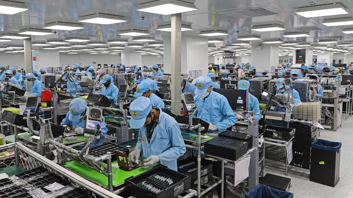
However, it's crucial to differentiate between a "pilot production line" and full-scale commercial manufacturing. Pilot lines are designed for testing processes, optimizing yields, and demonstrating feasibility, but they are a long way from the mass production required to compete with established silicon foundries like TSMC or Samsung. The journey from lab to fab is notoriously difficult, fraught with challenges in defect density, cost-effectiveness, and integration into existing manufacturing ecosystems.
North American policymakers and industry leaders will undoubtedly consider this claim within the broader context of semiconductor self-sufficiency and technological sovereignty. It underscores the importance of continued investment in fundamental materials science, advanced manufacturing techniques, and a skilled workforce to maintain a competitive edge. The ability to innovate and scale new materials quickly could become a decisive factor in who leads the next wave of technological innovation.
The establishment of an 8-inch 2D semiconductor pilot line, if verified and scalable, represents a significant marker in the global race for next-generation computing. While the road to widespread commercial adoption for 2D materials is still long and filled with formidable engineering and economic hurdles, this announcement from a Chinese startup serves as a powerful reminder that the future of electronics is constantly being rewritten, potentially ushering in an era of devices that are smaller, faster, and more efficient than anything we can imagine with today's silicon.
Frequently asked questions
What is the key claim made by the Chinese startup?
The Chinese startup claims to have established the world's first 8-inch pilot production line for two-dimensional (2D) semiconductors. This represents a significant advancement in semiconductor manufacturing and post-silicon electronics.
What are 2D semiconductors?
Two-dimensional (2D) semiconductors are materials with atomic-scale thickness, offering unique electronic properties superior to traditional silicon. They are crucial for developing smaller, more efficient electronic devices.
How does this impact the semiconductor industry?
This development could revolutionize the global semiconductor industry by paving the way for post-silicon electronics. It signifies a move towards next-generation computing and device manufacturing.
What products could benefit from this technology?
This technology could significantly impact various products, including future smartphones, advanced AI systems, high-performance computing, and other consumer electronics requiring greater efficiency and power.
Why is an 8-inch production line significant?
An 8-inch pilot production line is significant because it demonstrates scalability and industrial viability. It's a crucial step from laboratory research to mass production, indicating readiness for commercial application.
Is this technology a replacement for silicon?
While not a direct replacement yet, 2D semiconductors represent a strong candidate for post-silicon electronics. They offer performance advantages that could eventually surpass silicon in specific applications, driving future innovation.